Patching my guitar amp's firmware
Contents
I’m having a lot of fun with reverse engineering lately, so when I was looking over the service manual for my guitar amp, a Yamaha THR10c, and saw references to a UART header in the schematic, I got excited. I wondered if anything cool was hiding in there. Next to it was a JTAG header. I knew next to nothing about JTAG, but had heard the name before associated with hardware hacking, so maybe that would be useful as well.
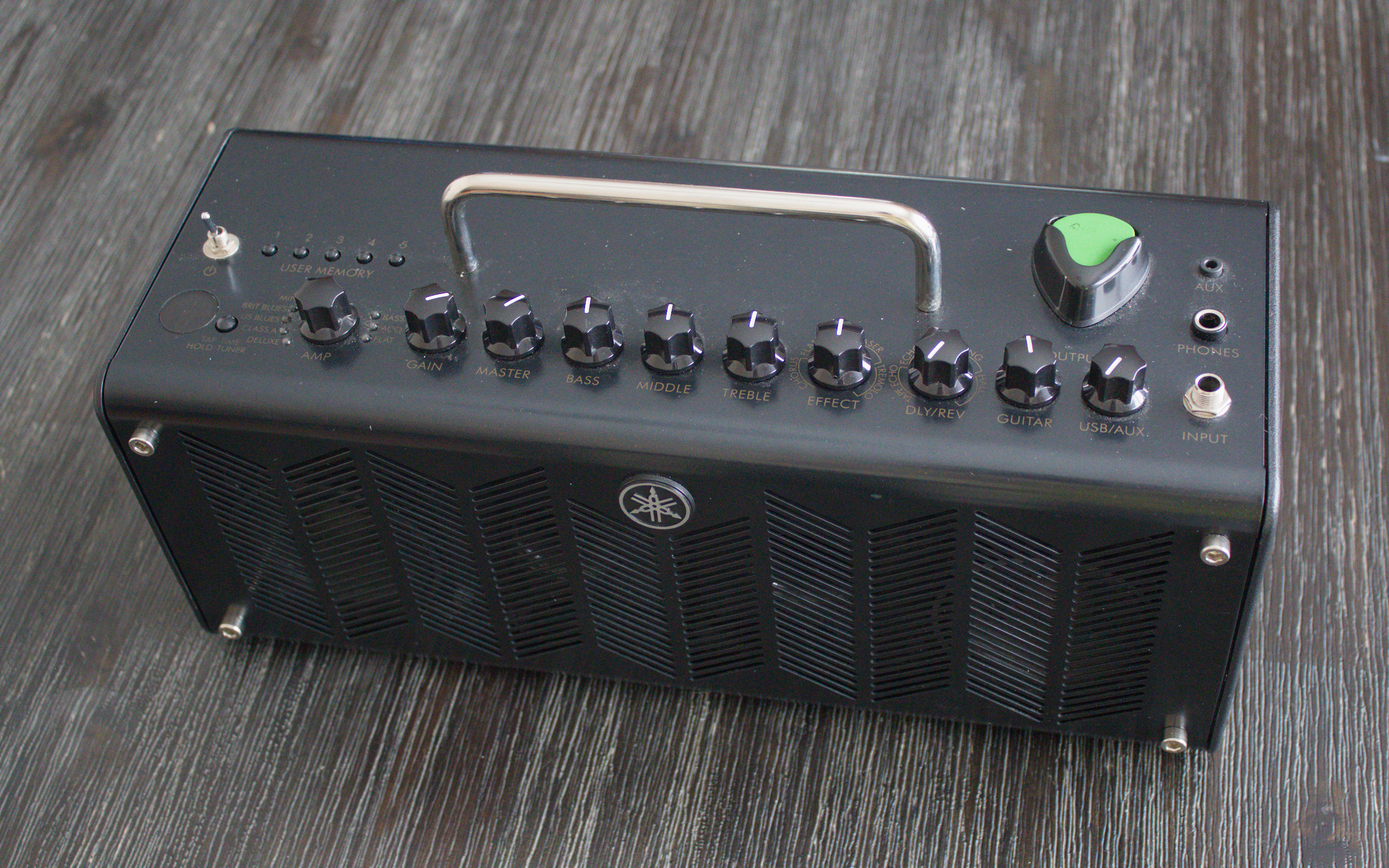
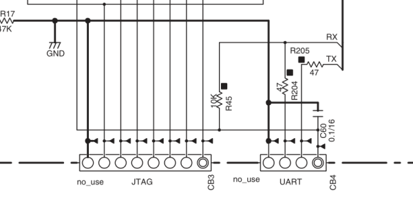
I had a few ideas of some changes I wanted to make to the firmware, so my main goal with this project was to find a way to dump the firmware and reflash the amp with a modified firmware.
One initial idea I had in mind was to add a way to toggle the guitar speaker simulation on and off so I could hook it up to real guitar speakers (either through a modification to add speaker out jacks, or hooking it up to a TPA3118 power amp module). While not officially supported, you can do this in the stock firmware by using a computer or phone to send a special MIDI SysEx command over USB. However, the speaker simulation reverts back to normal when you change the amp model, and the volume is raised considerably as a side-effect.
Another thing I wanted was a mode where the internal speaker would play even when the headphone port was connected (for instance, to additional speakers or a mixer).
Hardware
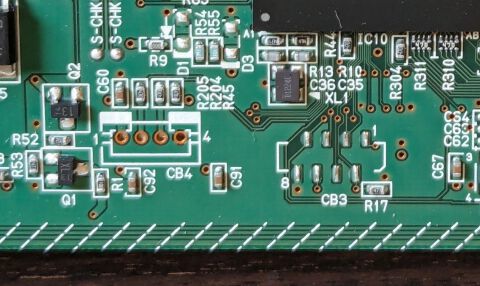
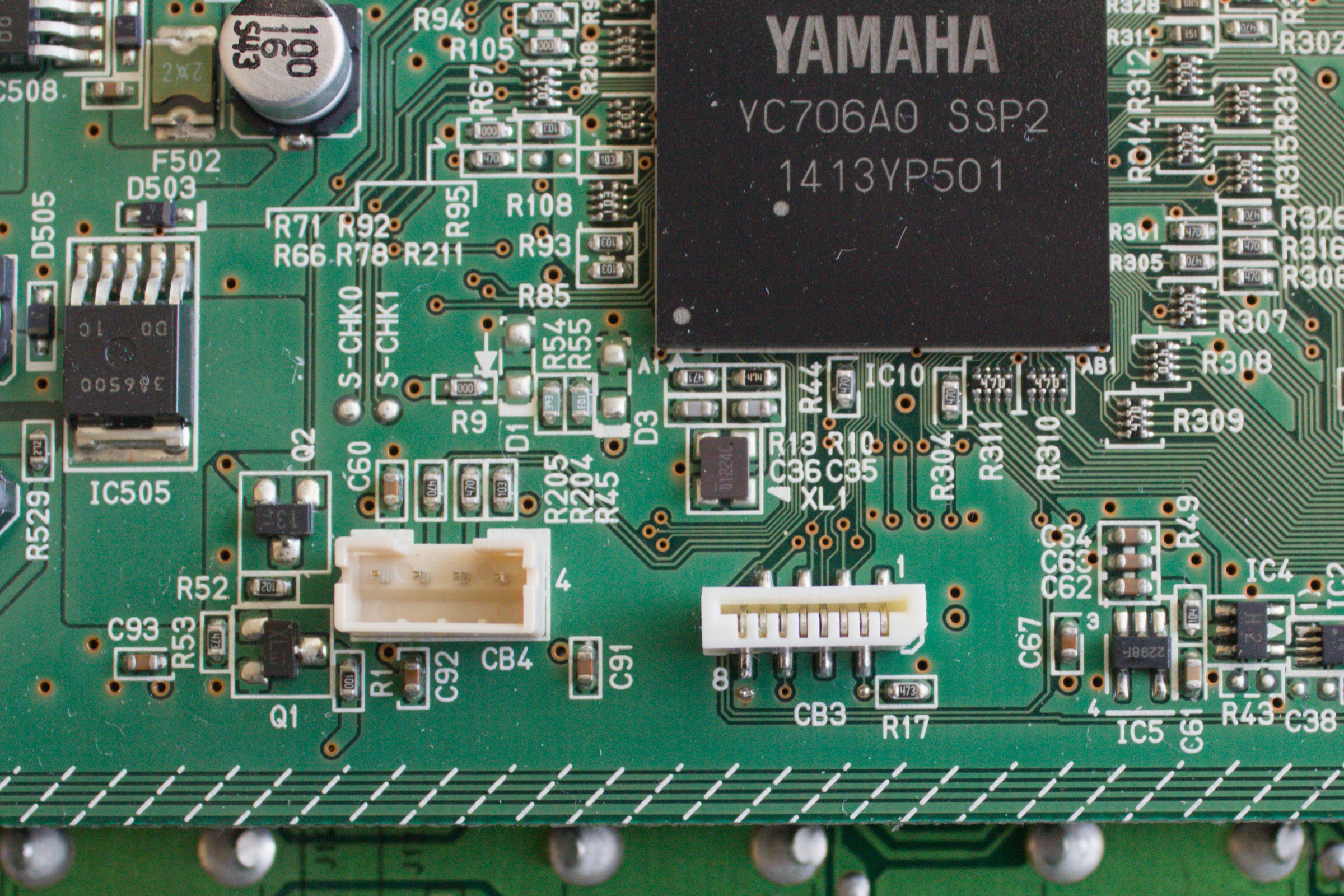
I opened up the amp as described in the service manual and located CB3 and CB4 on the main PCB.
Identifying and soldering the connectors
It seemed easy enough to solder on connectors to these headers, I just needed to identify which connectors to use. I measured the pin pitch of CB4 at 2mm, and CB3 at 1mm. The UART connector was pretty easy to identify as from the JST PH series (B4B-PH-K).
The JTAG connector wasn’t so obvious to me. Was it two staggered rows of 2mm pitch or one row of 1mm pitch with staggered contacts? I searched through online connector identifiers, as well as DigiKey and Mouser product indexes, but I didn’t find anything that seemed to match. I eventually noticed a similar footprint on another part of the board that used an flat flexible cable (FFC). This is why I hadn’t found it before; I didn’t think to look through FFC connectors. I saw a JST marking on that one, and I believe it is from the FMN series. Mouser didn’t have the 8-pin reverse version in stock (08FMN-BMTTR-A-TB), so I went with the compatible Molex 52808-0870.
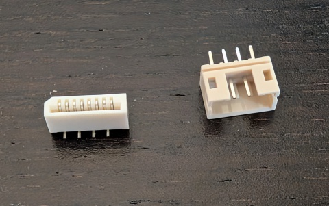
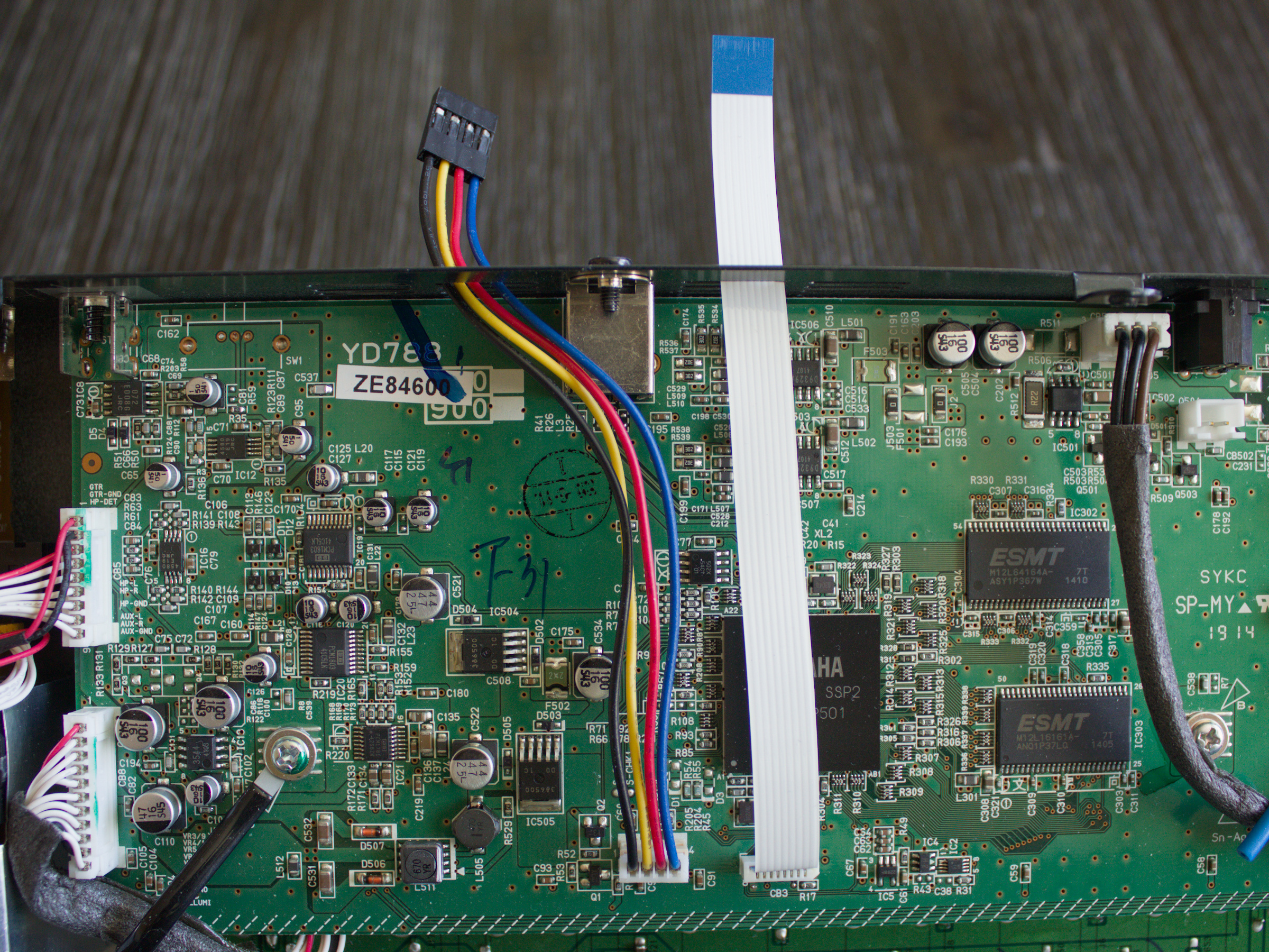
Once I received the new connectors in the mail, I removed the main PCB from the case and then cleared the CB4 through-holes with a solder pump. This was a bit tricky for the ground pin, which conducts heat to the ground plane very easily, but with some patience I eventually got it all clean. I then soldered on the new connectors. I don’t have much experience with SMD soldering, so CB3 gave me some trouble, but I’m happy with how it turned out.
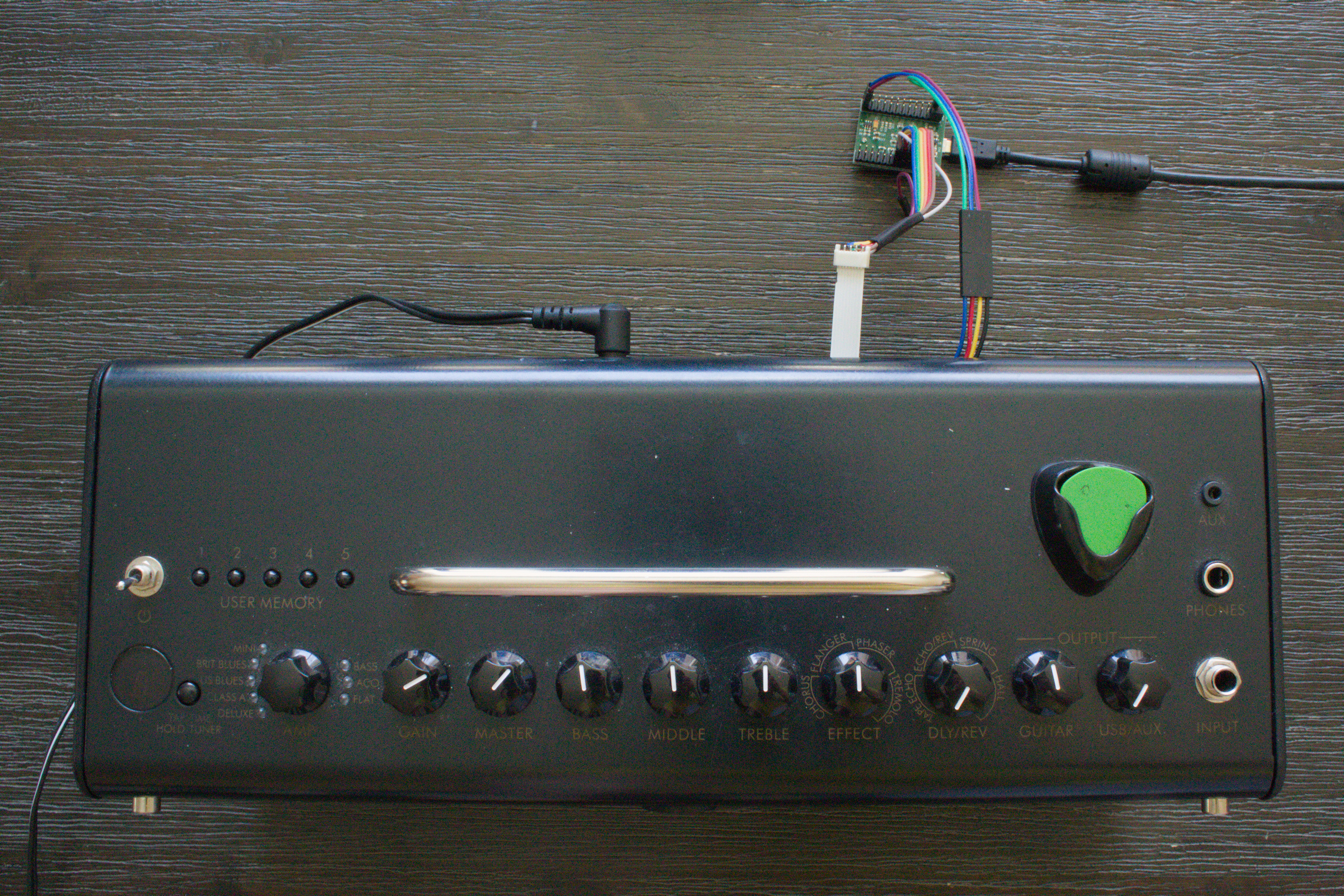
I fed cables for the two new connectors though slots at the back of the amp so I could close it up and still use it while working on this project.
Testing the UART
Now that I had connectors in place I hooked it up to my computer using a USB-UART cable and powered on the amp. Unfortunately, nothing was printed at all. I tried a bunch of different common baud rates and still nothing. I confirmed with an oscilloscope that there was no activity on TX.
Well, that’s a bummer. Maybe I’ll have better luck with JTAG.
JTAG
After reading more about JTAG and what it’s used for, it seemed quite promising. JTAG is a serial interface designed for hardware testing, and is commonly used for debugging embedded processors. It has four main pins, TCK, TMS, TDI, and TDO, which are used to interact with a state machine called a TAP controller. TCK, TMS, and TDI are all outputs from your JTAG adapter; TMS is used to navigate the state machine, TDI provides data input, and TCK is a clock which samples the inputs and advances to the next state. TDO is an output from the TAP controller and provides data output. Optionally, there is also a TRST pin used to reset the controller.
There are lots of diagrams showing the TAP state machine available online, and I think having a basic mental model was helpful for getting started.
One of the best resources I found was a post by wrongbaud, which walked through the whole process of using JTAG with a device you know nothing about.
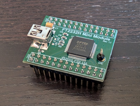
It seems that the most popular and well supported JTAG adapters are the FTDI FT2232H-based ones. One benefit of this chip is it has two multi-purpose channels, so I can use JTAG on one and UART on the other (assuming I could get it working). There are lots of options available here, but most of the links to these products from the UrJTAG and OpenOCD documentation were dead. I went with the FTDI FT2232H Mini Module.
The JTAG header (CB3) on my amp had 8 pins, most of which were connected directly to a labeled pin on the SSP2 (the main chip of the amp) so I didn’t have to go through the process of discovering the mapping myself. There was one pin that went into an AND gate and then to a pin labeled ICN on the SSP2. The other input to the gate was the output of an R3112N291A-TR-F IC. This appears to be some sort of low voltage detector, and the datasheet mentions that it can be used for system reset, which seemed likely.
On the FT2232H, AD0-AD3 are used for TCK, TDI, TDO, and TMS respectively. AD4-7 are regular GPIO pins and are configured in software. When I first connected my amp to the mini module, I did not connect the reset pins, which turned out to be a problem: TRST is active-low and pulled to ground by R17, so to enable the TAP controller it needs to be set high. This can be done by connecting TRST to VCC, but to allow the JTAG software to reset the TAP controller, we can use the GPIO pins on the mini module. I used AD4 for TRST and AD5 for SRST.
| CB3 Pin | Mini Module Pin | Description |
|---|---|---|
| 1 | VCC | |
| 2 | CN2-14 (AD4) | TRST |
| 3 | CN2-10 (AD1) | TDI |
| 4 | CN2-12 (AD3) | TMS |
| 5 | CN2-7 (AD0) | TCK |
| 6 | CN2-9 (AD2) | TDO |
| 7 | CN2-13 (AD5) | SRST |
| 8 | CN2-6 | GND |
I hooked all this up to a 2x5 header, along with a jumper wire from V3V3 to VIO as described in the mini module datasheet. I also added a jumper from CN3-1 to CN3-3 to use USB bus-power for the FT2232H.
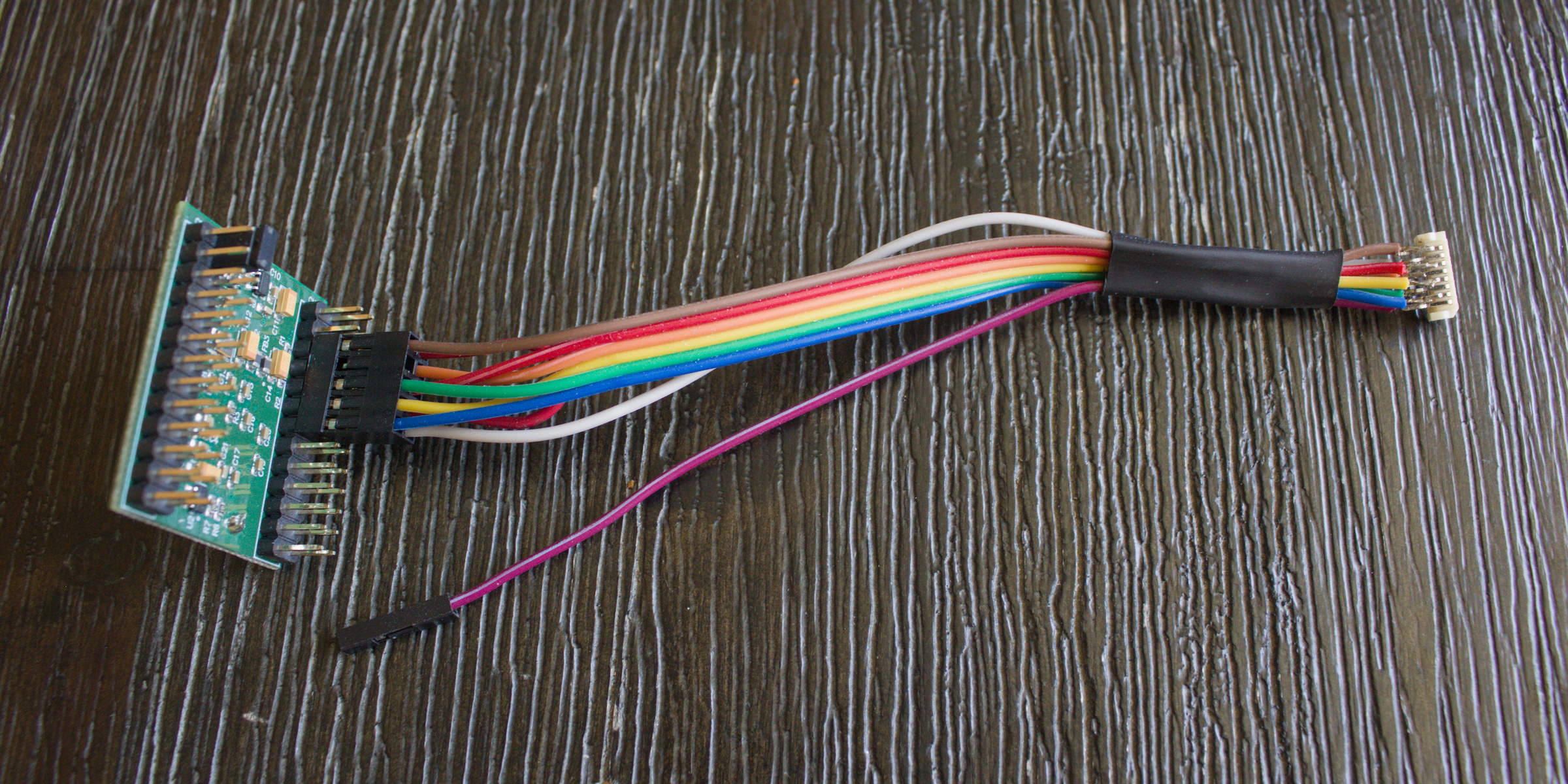
Here’s the amp all closed up with JTAG and UART hooked up to the mini module.
Software
Now that all the hardware bits were in place, I could start using software like OpenOCD and UrJTAG to interact with my amp over JTAG. I first tried UrJTAG as suggested by wrongbaud, but ran into some trouble with the TRST pin since it was not configurable. I did get it working by tying it to VCC, but I think it would have been easier to go straight to OpenOCD.
Configuring OpenOCD
The default interface/ftdi/minimodule.cfg script from OpenOCD
does not set up TRST either, but it can be configured with a custom
script.
adapter driver ftdi
ftdi device_desc "FT2232H MiniModule"
ftdi vid_pid 0x0403 0x6010

ftdi layout_init 0x0008 0x000b
ftdi layout_signal nTRST -data 0x0010 -oe 0x0010
ftdi layout_signal nSRST -data 0x0020 -oe 0x0020
I launched OpenOCD with openocd -f minimodule.cfg -c 'transport select jtag', and was happy to see it had discovered the TAP
controller.
Warn : There are no enabled taps.  AUTO PROBING MIGHT NOT WORK!!
Info : JTAG tap: auto0.tap tap/device found: 0x4f1f0f0f (mfg: 0x787 (<unknown>), part: 0xf1f0, ver: 0x4)
I searched around for the JTAG ID 4F1F0F0F, which seemed to be commonly used by the NXP LPC 2xxx series, which are based on an ARM7TDMI-S core.
It seemed like a reasonable assumption that the SSP2 also used an ARM7TDMI-S core, so I started an OpenOCD config file.
transport select jtag
jtag newtap ssp2 cpu -irlen 4 -expected-id 0x4F1F0F0F

target create ssp2.cpu arm7tdmi -chain-position ssp2.cpu

reset_config trst_and_srst
Indeed, it seemed to work. openocd -f minimodule.cfg -f thr10.cfg
started with the message saying it had detected EmbeddedICE version
7, which provides debug support for ARM7 cores. I was now able to
connect with gdb using gdb -ex 'target extended-remote :3333' and
read and write memory and registers, as well as step through the
code the processor was executing!
However, the default of little-endian was not correct for this target. ARM7TDMI cores can run in big-endian or little-endian depending on an input pin, and it was clear that the SSP2 used big-endian by comparing memory read byte-by-byte against memory read word-by-word:
(gdb) x/8xb 0
0x0:	0xe3	0xa0	0xf4	0x02	0xe5	0x9f	0xf0	0x18
(gdb) x/2xw 0
0x0:	0xe3a0f402	0xe59ff018
I went back to update the config file to correct the endianness.
While I was here, I bumped the JTAG adapter speed to 2000 KHz since
the THR10 uses a 12.288 MHz clock and the OpenOCD documentation
suggests at most one sixth of the CPU clock. I also added -ircapture 0x1 -irmask 0xF based on the ARM7TDMI reference manual; the TAP
instruction register is 4 bits wide and upon entering the CAPTURE-IR
state it is loaded with 0x1. These parameters are used by OpenOCD
to verify that JTAG is operating correctly. Finally, I found I also
needed adapter srst delay 100 to get system reset to work.
transport select jtag
jtag newtap ssp2 cpu -irlen 4 -expected-id 0x4F1F0F0F -ircapture 0x1 -irmask 0xF

target create ssp2.cpu arm7tdmi -chain-position ssp2.cpu -endian big

adapter speed 2000
adapter srst delay 100
reset_config trst_and_srst
The GDB target description format doesn’t indicate the target
endianness, so I had to configure gdb for big-endian as well. I did
this with a file containing startup commands. I also enabled
disassemble-next-instruction, which was quite helpful for following
what was going on.
target extended-remote :3333
set endian big
set disassemble-next-instruction on
Now, I could launch gdb with gdb -x thr10.gdb and everything gets
configured correctly.
Dumping the address space
In order to start analyzing the firmware, I needed to dump it to a
file. After poking around for a bit, there seemed to some code at
address 0 as well as at 0x2000000. The first instruction excecuted
at the reset vector (address 0) was a jump to 0x2000000. According
to the schematic, the THR10 has a 2 MiB flash, so under the assumption
that one of these addresses was the start of the flash, I dumped
0x0000000-0x4000000 (64 MiB) of the address space to memory.bin,
which should be more than enough for everything I was interested
in at the moment.
(gdb) starti
(gdb) dump memory memory.bin 0 0x4000000
This was a bit slow and took around 15 minutes to complete.
Firmware disassembly and analysis
I loaded memory.bin into Ghidra as an ARM:BE:32:v4t:apcs raw
binary and started analyzing it. The first thing it does after
jumping to 0x2000000 is copy 0x10000 bytes (64 KiB) from 0x2000100
to 0x4000000 and then jump to it.
At just before 0x2010000, there is what looks like a build
timestamp and executable identifier DTAb.
0200ffd0: 41 75 67 20 32 30 20 32 30 31 32 00 00 00 00 00  Aug 20 2012.....
0200ffe0: 30 39 3a 33 39 3a 33 36 00 00 00 00 00 00 00 00  09:39:36........
0200fff0: 44 54 41 62 ff ff ff ff ff ff ff ff ff ff ff ff  DTAb............
There is a similar timestamp and identifier at 0x2110000.
0210ffd0: 41 75 67 20 20 33 20 32 30 31 32 00 00 00 00 00  Aug  3 2012.....
0210ffe0: 31 31 3a 32 36 3a 35 30 00 00 00 00 00 00 00 00  11:26:50........
0210fff0: 44 54 41 6d ff ff ff ff ff ff ff ff ff ff ff ff  DTAm............
At this point I realized I was dealing with two separate program
images. DTAb is the bootloader, and DTAm is the main firmware
image.
At 0x2010000 (the start of DTAm), there is some similar looking
code to what was copied to 0x4000000 (the start of DTAb). It sets
up stack pointers for the different ARM exception modes, and then
zeros 128 KiB at 0x1000000 at 256 KiB at 0x4000000. These seemed
likely to be RAM regions, which made sense since there are two
SDRAM chips on the main board. After that, it makes a sequence of
calls to functions I’ve annotated as copywords and zerowords.
These set up different data and bss segments of the program image.
02013868  mov  r0,#0xd2		               /* change to IRQ mode */
0201386c  msr  cpsr_c,r0
02013870  ldr  sp,[DAT_02013b10]  = 0101F9D0h  /* set stack pointer to 0x101F9D0 */
02013874  mov  r0,#0xd7                        /* change to Abort mode */
02013878  msr  cpsr_c,r0
0201387c  ldr  sp,[DAT_02013b14]  = 0101FBE0h  /* set stack pointer to 0x101FBE0 */
02013880  mov  r0,#0xdb                        /* change to Undefined mode */
02013884  msr  cpsr_c,r0
02013888  ldr  sp,[DAT_02013b18]  = 0101FBF0h  /* set stack pointer to 0x101FBF0 */
0201388c  mov  r0,#0xd1                        /* change to FIQ mode */
02013890  msr  cpsr_c,r0
02013894  ldr  sp,[DAT_02013b1c]  = 0101FC00h  /* set stack pointer to 0x101FC00 */
02013898  mov  r0,#0xd3                        /* change to Supervisor mode */
0201389c  msr  cpsr_c,r0
020138a0  ldr  sp,[DAT_02013b20]  = 0101FAD0h  /* set stack pointer to 0x101FAD0 */
undefined4 *ptr;

/* zero ram0 */
ptr = &DAT_01000000;
do {
	*ptr = 0;
	ptr = ptr + 1;
} while (ptr < &DAT_01020000);

/* zero ram1 */
ptr = &LAB_04000000;
do {
	*ptr = 0;
	ptr = ptr + 1;
} while (ptr < (undefined4 *)0x4040000);

copywords(&DAT_0208645c,0x4000000,&DAT_04010100);      /* ram1 .data */
zerowords(&DAT_04010100,&DAT_040219b4);                /* ram1 .bss */
copywords(&DAT_0209655c,&DAT_0101f1d0,&DAT_0101f9d0);  /* IRQ stack */
zerowords(&DAT_0101f9d0,&DAT_0101f9d0);
copywords(&DAT_02096d5c,&DAT_0101f9d0,&DAT_0101fad0);  /* Supervisor stack */
zerowords(&DAT_0101fad0,&DAT_0101fad0);
copywords(&DAT_02096e5c,&DAT_0101fad0,&DAT_0101fbd0);  /* User stack */
zerowords(&DAT_0101fbd0,&DAT_0101fbd0);
copywords(&DAT_02096f5c,&DAT_0101fbd0,&DAT_0101fbe0);  /* Abort stack */
zerowords(&DAT_0101fbe0,&DAT_0101fbe0);
copywords(&DAT_02096f6c,&DAT_0101fbe0,&DAT_0101fbf0);  /* Undefined stack */
zerowords(&DAT_0101fbf0,&DAT_0101fbf0);
copywords(&DAT_02096f7c,&DAT_0101fbf0,&DAT_0101fc00);  /* FIQ stack */
zerowords(&DAT_0101fc00,&DAT_0101fc00);
copywords(&DAT_02096f8c,&DAT_01008000,&DAT_0100bad0);  /* ram0 .data */
zerowords(&DAT_0100bad0,&DAT_01015f6c);                /* ram0 .bss */
At this point I was pretty confident that 0x2000000 was the flash. I believe the 8 KiB of low-level code and data at address 0 must be part of the SSP2 chip.
Great! I now had a pretty good understanding of the flash and memory layout of my amp.
| Address | Length | Description |
|---|---|---|
| 0x2000000 | 0x100 | Bootloader first stage |
| 0x2000100 | 0xFF00 | Bootloader (DTAb) |
| 0x2010000 | 0x100000 | Main firmware (DTAm) |
| Address | Length | Description |
|---|---|---|
| 0x0000000 | 0x1BE4 | .text.ssp2 |
| 0x1008000 | 0x3AD0 | .data.ram0 |
| 0x100BAD0 | 0xA49C | .bss.ram0 |
| 0x101F1D0 | 0x800 | IRQ stack |
| 0x101F9D0 | 0x100 | Supervisor stack |
| 0x101FAD0 | 0x100 | User stack |
| 0x101FBD0 | 0x10 | Abort stack |
| 0x101FBE0 | 0x10 | Undefined stack |
| 0x101FBF0 | 0x10 | FIQ stack |
| 0x101FC00 | 0x204 | .data.ssp2 |
| 0x101FE04 | 0x60 | .bss.ssp2 |
| 0x2010000 | 0x7645C | .text |
| 0x4000000 | 0x10100 | .data.ram1 |
| 0x4010100 | 0x118B4 | .bss.ram1 |
Of the 2 MiB flash, 1 MiB was used for DTAm. Since I’d found that 554 KiB were used for firmware code and data, around 470 KiB was left for me to use for my own code and data. This is more than enough for anything I had in mind.
Relinking the firmware
In order to add my own code to the firmware, I needed to turn the
flat firmware image into an ELF object so I could relink it. First,
I extracted just the DTAm portion of my memory dump into
thr10_ver104c_20120803.bin. Then, I used an assembly file to split
it into sections based on the memory layout I had discovered earlier.
.macro fwdata addr:req,size:req
	.incbin "thr10_ver104c_20120803.bin",\addr-0x2010000,\size
.endm

.text
	fwdata 0x2010000,0x7645C

.section .data.ram1,"aw"
	fwdata 0x208645C,0x10100
.section .bss.ram1,"aw",%nobits
	.space 0x00118B4

.data
	fwdata 0x2096F8C,0x03AD0
.bss
	.space 0x000A49C

.section .data.exc,"aw"
	fwdata 0x209655C,0x00800	/* irq */
	fwdata 0x2096D5C,0x00100	/* svc */
	fwdata 0x2096E5C,0x00100	/* usr */
	fwdata 0x2096F5C,0x00010	/* abt */
	fwdata 0x2096F6C,0x00010	/* und */
	fwdata 0x2096F7C,0x00010	/* fiq */

.section .fwinfo,"a"
	fwdata 0x210FFD0,0x00030
I wrote a linker script to place these sections where the firmware
expects them. I also added sections .text.patch, .rodata.patch,
.data.patch, .bss.patch and defined symbols for their size and
address. I’ll use these later for my own code. I decided to start
my code and data at 0x20A0000, a nice round address, to make it
easy to identify.
MEMORY
{
	ram0 (w) : ORIGIN = 0x1000000, LENGTH = 0x0020000
	rom (rx) : ORIGIN = 0x2000000, LENGTH = 0x0200000
	ram1 (w) : ORIGIN = 0x4000000, LENGTH = 0x0040000
}

SECTIONS
{
	.text       0x2010000 : { thr10*.o(.text)     } >rom
	.data.ram1            : { thr10*.o(.data.dsp) } >ram1 AT>rom
	.bss.ram1             : { thr10*.o(.bss.dsp)  } >ram1
	.data.exc   0x101F1D0 : { thr10*.o(.data.exc) } >ram0 AT>rom
	.data       0x1008000 : { thr10*.o(.data)     } >ram0 AT>rom
	.bss                  : { thr10*.o(.bss)      } >ram0

	.text.patch 0x20A0000 : { *(.text)            } >rom
	.rodata.patch         : { *(.rodata)          } >rom
	.data.patch           : { *(.data)            } >ram0 AT>rom
	.bss.patch            : { *(.bss)             } >ram0

	.fwinfo     0x210FFD0 : { *(.fwinfo)           } >rom
}

__data_patch      = ADDR(.data.patch);
__data_patch_load = LOADADDR(.data.patch);
__data_patch_size = SIZEOF(.data.patch);
__bss_patch       = ADDR(.bss.patch);
__bss_patch_size  = SIZEOF(.bss.patch);
Now, if I split the raw firmware into an ELF object, relink it with this script, then extract the raw image, I should get back exactly what I started with.
$ armeb-none-eabi-as -o thr10_ver104c_20120803.o thr10_ver104c_20120803.s
$ armeb-none-eabi-ld -o thr10_ver104c_20120803.elf -T thr10.ld thr10_ver104c_20120803.o
$ armeb-none-eabi-objdump -h thr10_ver104c_20120803.elf

thr10_ver104c_20120803.elf:     file format elf32-bigarm

Sections:
Idx Name          Size      VMA       LMA       File off  Algn
  0 .text         0007645c  02010000  02010000  00001000  2**0
                  CONTENTS, ALLOC, LOAD, READONLY, CODE
  1 .data.exc     00000a30  0101f1d0  0209655c  000881d0  2**0
                  CONTENTS, ALLOC, LOAD, DATA
  2 .data         00003ad0  01008000  02096f8c  00089000  2**0
                  CONTENTS, ALLOC, LOAD, DATA
  3 .bss          0000a49c  0100bad0  0209aa5c  0008cad0  2**0
                  ALLOC
  4 .fwinfo       00000030  0210ffd0  0210ffd0  0008cfd0  2**0
                  CONTENTS, ALLOC, LOAD, READONLY, DATA
  5 .ARM.attributes 00000014  00000000  00000000  0008d000  2**0
                  CONTENTS, READONLY
  6 .data.ram1    00010100  04000000  0208645c  00078000  2**0
                  CONTENTS, ALLOC, LOAD, DATA
  7 .bss.ram1     000118b4  04010100  0209655c  00089100  2**0
                  ALLOC
$ armeb-none-eabi-objcopy -O binary -j '.text*' -j '.data*' -j '.fwinfo' \
	--gap-fill 0xFF --pad-to 0x2100000 \
	thr10_ver104c_20120803.elf thr10_ver104c_20120803-relinked.bin
$ cmp thr10_ver104c_20120803.bin thr10_ver104c_20120803-relinked.bin
$
Nice! Now I can easily add my own objects to the linker command-line to build them into the firmware image.
This ELF file also made analysis in Ghidra a lot easier now that the sections were labeled and loaded at the correct address.
Patching the firmware
I now needed a way to patch small parts of the original firmware to hook into my own code. I wasn’t sure if there is a more standard way to do this, but the approach I used ended up working out pretty well.
In the assembly file, I added a new section .patch.text which
mirrors the target section .text. Each symbol represents a patch
which will be copied over the original .text. I wrapped this up
into a couple of macros.
.macro patch addr:req,body:vararg
	.section .patch.text,"xo",.text
	.org \addr-0x2010000
	patch\+:
	.ifnb \body
		\body
		endpatch
	.endif
.endm

.macro endpatch
	.size patch\+,.-patch\+
.endm
Although I had set up data and bss segments for my own code, I still
needed to initialize them at start up, like the firmware did for
its data. I noticed that the data for the exception stacks was all
zero, and the ram was already zero initialized earlier, so I
repurposed one pair of these copywords/zerowords calls by
patching the address constants with the symbols I had defined in
the linker script earlier.
patch 0x2013BA8	.word __data_patch_load  /* was: FIQ data LMA */
patch 0x2013BAC	.word __data_patch       /* was: FIQ data VMA */
patch 0x2013BB0	.word __data_patch_size  /* was: FIQ data size */
patch 0x2013BB4	.word __bss_patch_size   /* was: FIQ bss size */
patch 0x2013BB8	.word __bss_patch        /* was: FIQ bss LMA */
To apply these patches, I wrote a small tool using libelf. It looks
for sections named .patch.*, and then for each symbol in that
section, copies it over on top of the original section (.text in
this case). Then, it changes the sh_info member of the corresponding
relocation section header to the original section so that relocations
are applied to the patched section.
Finally, I removed the .patch.* sections since they are no longer
needed.
$ cp thr10_ver104c_20120803.o thr10.o.tmp
$ tools/patchfirmware thr10.o.tmp
$ armeb-none-eabi-objcopy -R '.patch.*' thr10.o.tmp thr10.o
$
After updating my Makefile to apply patches with my tool before
linking, I could build new custom firmware images using make.
More firmware analysis
From here, the next step was a deep dive into the firmware with Ghidra to start to build an understanding of how it worked. At first, not much made sense, but the more I figured out, the more context I had, and the pieces gradually started to fall into place.
One initial problem I encountered was that many function calls were made using these helper functions to facilitate the transition between the ARM and Thumb instruction sets. This made analysis much more difficult since it broke Ghidra’s cross-reference analysis.
 2010628:	4700      	bx	r0
 201062a:	4708      	bx	r1
 201062c:	4710      	bx	r2
 201062e:	4718      	bx	r3
 2010630:	4720      	bx	r4
 2010632:	4728      	bx	r5
 2010634:	4730      	bx	r6
 2010636:	4738      	bx	r7
The helper used depends on the number of arguments to the function.
For example, to call a 3-argument ARM function from a Thumb function,
the call site moves the arguments into r0-r2 like normal, the
function address into r3, then emits bl 0x201062e. Then the helper
branches to the target function with bx r3, which changes the
instruction set according the the least significant bit in the
address. Instructions are always aligned to a multiple of 2, so
this bit is otherwise unused. The reason for this indirection is
that ARMv4 does not have a blx instruction, so setting LR and
exchanging instruction sets must be done in two separate steps.
This is a slightly different approach to how the GNU toolchain does
it. Instead, the GNU linker will emit stubs for functions called
across different instruction sets, (for example, __f_from_thumb
to call f, an ARM function, from a Thumb function). These stubs
switch the instruction set, and then jump to the target function.
To fix the cross-references, I wrote a Ghidra script to loop over each call to these bx helpers, check if the address in the corresponding register was a constant, and if so add a function call reference to that address. This made it a lot easier to determine the list of callers of any given function.
After a whole bunch of analysis, annotation, and staring at decompiled code in confusion, I found a lot of interesting stuff:
- The firmware runs several different threads for different purposes. For example, one handles USB MIDI, and another deals with panel I/O (LEDs, potentiometers, buttons). They can wait for and post events to other threads.
- The DSP runs independently of the main ARM core. Even when it was interrupted for debugging, the amp still played my guitar input.
- There is a memory region at 0x7000000 for memory mapped I/O. I found the buttons (0x7001D60) and potentiometers (0x7001800) by dumping the I/O space before and while the buttons were pressed or potentiometers were changed and looking for differences.
- I found the UART with a similar process. Under the assumption that the firmware initialized it at startup, I wrote random bytes at different common baud rates and dumped and compared the I/O space. Eventually I started to see one address (0x7002001) change as I narrowed in on the correct baud rate of 38400. I managed to send characters the other direction by writing to the adjacent address (0x7002000) from gdb. By following references to these addresses, I found that there was already code dealing with buffering input and output to the UART; it was just unused.
- I identified a bunch of software floating point routines, including
basic arithmetic, conversion to and from integer types, trigonometry,
log, power, and sqrt. Rather than trying to understand the code
itself, which was very complex, I identified these by running the
code in qemu-user with a variety of different inputs to see what
outputs they gave. For example, if the function called with 2
resulted in 1.414, that was pretty good evidence it was
sqrt. - I found a SysEx command in the bootloader that can be used to dump the firmware over USB MIDI in the same format that is used to update the device firmware. This was a really nice find since it means that you don’t have to do any hardware modification to dump and flash new firmware.
Making my changes
To achieve my goal of adding a mechanism to toggle speaker cabinet simulation and to force the internal speaker output, I needed to interpose my own routine to handle button presses and find a way to indicate whether these modes were on or off. And of course I needed to find out how to actually select the cabinet simulation type and mute/unmute the speaker.
Buttons
To toggle these new modes, I had a few options. The THR10 has six buttons, one for setting effect tempo and toggling tuner mode, and the other 5 for loading and storing presets. Looking at the top panel circuit, it used 4 cycling pulse outputs (SCN0, SCN2, SCN4, SCN6) and 7 input/outputs (SDT0-SDT6). When SCN0 was high, SDT0-SDT6 were configured as inputs and the amp read the button state. When SCN2, SCN4, or SCN6 were high, SDT0-SDT6 were configured as outputs, controlling 3 sets of 7 LEDs.
Since the amp only used 6 buttons out of the possible 7, it actually had room for one more switch input by adding a diode and switch between SCN0 and SDT6.
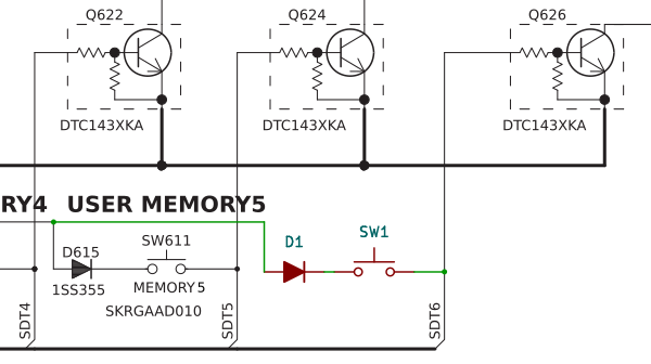
I confirmed that I was able to read an additional switch as the next highest bit at 0x7001D60. However, to avoid requiring hardware modification, I opted to use a combination of the existing buttons: holding TAP while pressing PRESET1 or PRESET2 to toggle bypass mode or force speaker mode respectively. This worked out quite nicely since it didn’t interfere much with the existing functions of the TAP button (which requires it to be held for a certain period of time, or tapped at a tempo).
I found that the function that handled button changes was at 0x2028CB8, and was called in only one location from thread 6. This was the function I needed to wrap to implement the new behavior. I patched the single call site to call my wrapper instead.
.thumb
patch 0x202BFA4	bl wrap_control_handle_buttons
LEDs
Similar to the buttons, the amp used only 19 out of the possible 21 outputs for LEDs: 8 for the amp modes, 7 for the 7-segment display, 3 for the tuner, and 1 for the sharp symbol. I could add up to two more LEDs for my own purposes by connecting them with a resistor between SCN4 and SDT6, as well as SCN6 and SDT6.
Again, I chose to avoid requiring hardware modification and reused the tuner LEDs, which were inactive when the amp was in normal operation. I used the left and right arrows to indicate cabinet simulation bypass, and the center dot to indicate that speakers were forced on.
Building an API
I eventually found everything I needed to implement my changes, so I started a header to expose a small API I could use in my own code.
/**** panel i/o ****/

enum panel_button {
        PANEL_BUTTON_TAP     = 0x01,
        PANEL_BUTTON_PRESET1 = 0x02,
        PANEL_BUTTON_PRESET2 = 0x03,
        PANEL_BUTTON_PRESET3 = 0x04,
        PANEL_BUTTON_PRESET4 = 0x05,
        PANEL_BUTTON_PRESET5 = 0x06,
};

/* returns a bitmask of the currently pressed buttons in `buttons` */
int panel_get_buttons(unsigned short *buttons);

enum panel_led {
	PANEL_LED_AMP0       = 0,
	PANEL_LED_AMP1       = 1,
	PANEL_LED_AMP2       = 2,
	PANEL_LED_AMP3       = 3,
	PANEL_LED_AMP4       = 4,
	PANEL_LED_AMP5       = 5,
	PANEL_LED_AMP6       = 6,
	PANEL_LED_AMP7       = 7,
	PANEL_LED_TUNELEFT   = 8,
	PANEL_LED_TUNECENTER = 9,
	PANEL_LED_TUNERIGHT  = 10,
	PANEL_LED_SHARP      = 11,
};

/* sets the state of an led */
void panel_set_led(int led, int off);

/**** control ****/

void control_handle_buttons(void);
void control_set_speaker(int on);

extern bool control_headphone_connected;

/**** amp emulation ****/

enum amp_cab {
	AMP_CAB_BRITBLUES_2x12  = 0,
	AMP_CAB_BOUTIQUE_2x12   = 1,
	AMP_CAB_CALIFORNIA_1x12 = 2,
	AMP_CAB_AMERICAN_1x12   = 3,
	AMP_CAB_BOUTIQUE_1x12   = 4,
	AMP_CAB_YAMAHA_2x12     = 5,
	AMP_CAB_NONE            = 6,
};

/* source of settings change */
enum amp_change_source {
	AMP_CHANGE_MIDI   = 0,  /* MIDI SysEx request */
	AMP_CHANGE_PANEL  = 1,  /* interaction with the top panel */
	AMP_CHANGE_PRESET = 2,  /* preset loaded */
	AMP_CHANGE_INIT   = 3,  /* amp initialized */
};

/* sets the speaker cabinet emulation type */
int amp_set_cab(int type, int source);

struct amp_state {
	unsigned char type;
	unsigned char gain;
	unsigned char master;
	unsigned char bass;
	unsigned char middle;
	unsigned char treble;
	unsigned char cab;
};

extern struct amp_state amp_state;

/**** tuner ****/

extern unsigned short tuner_active;
I added symbols to thr10_ver104c_20120803.s for all the functions
and objects I had declared in thr10.h.
.macro def type:req,addr:req,size:req,name:req
	.globl \name
	.set \name,\addr
	.type \name,\type
	.size \name,\size
.endmacro

def %function 0x201E598+1   16 panel_get_buttons
def %function 0x201E72C+1  102 panel_set_led

def %function 0x2028CB8+1 3488 control_handle_buttons
def %function 0x2017380+1   12 control_set_speaker
def %object   0x1012614      1 control_headphone_connected

def %function 0x201AF88+1  584 amp_set_cab
def %object   0x4021904     16 amp_state

def %object   0x101260C      2 tuner_active
My code
Finally, I was ready to implement my new features!
#include "thr10.h"

static bool cab_bypass;
static bool force_speaker;

void
wrap_control_handle_buttons(void)
{
	static unsigned short button_save;
	static unsigned short wait_release;
	unsigned short button, button_prev;

	panel_get_buttons(&button);
	button_prev = button_save;
	button_save = button;
	if (wait_release) {
                /*
                if we intercepted our special button combination,
                wait until all buttons are released before reverting
                back to the original button handler
		*/
		if (button)
			return;
		wait_release = false;
	}
	if (button & button_prev & PANEL_BUTTON_TAP) {  /* TAP held */
		button &= ~button_prev;
		if (button & PANEL_BUTTON_PRESET1) {
			cab_bypass = !cab_bypass;
			panel_set_led(PANEL_LED_TUNE_LEFT, !cab_bypass);
			panel_set_led(PANEL_LED_TUNE_RIGHT, !cab_bypass);
			amp_set_cabinet(cab_bypass ? AMP_CAB_NONE : amp_state.cabinet, AMP_CHANGE_PANEL);
			wait_release = true;
			return;
		}
		if (button & PANEL_BUTTON_PRESET2) {
			force_speaker = !force_speaker;
			panel_set_led(PANEL_LED_TUNE_CENTER, !force_speaker);
			control_set_speaker(force_speaker || !control_get_headphone_connected());
			wait_release = true;
			return;
		}
	}
	/* defer to original button handler */
	control_handle_buttons();
}
That was simple enough, but I wasn’t done just yet. Currently, I had set it up so that pressing the special button combinations had the desired effect, but these settings did not persist when the amp type was changed, or when the headphone cable was connected or disconnected. I needed to find where those changes were made and make them aware of my two new new modes.
For the force speaker mode, this was easy. I found where the firmware
called control_set_speaker in response to the headphones getting
connected or disconnected, and patched it to call a wrapper instead.
void
wrap_control_set_speaker(int on)
{
	control_set_speaker(on || force_speaker);
}
patch 0x202BF4A bl wrap_control_set_speaker
Unfortunately, this was a bit more involved for the speaker simulation,
since amp_set_cab was not used when a new amp type was selected.
Instead, it used a lower level function I called dsp_command which
is used to program and set parameters for blocks on the DSP.
The parameters are passed through a struct, and while I still don’t understand it very well, I managed to figure out the basics. The following is my best guess of how it works, using various terms I invented for different things based on my limited understanding.
union dsp_command {
	struct {
		unsigned short block;
	        unsigned char type;  /* 0=setblock, 1=setparam 1, 2=setparam 2 */
	};
	struct {
		unsigned short block;
		unsigned char type;
		unsigned char param;
		unsigned short value;
	} setparam;
	struct {
		unsigned short block;
		unsigned char type;
		unsigned char flags;  /* 2=no params1, 4=no params2 */
		unsigned short id;
		unsigned short numparams1;
		unsigned short field5;
		unsigned short *params1;
		unsigned short *params2;
	} setblock;
};

int dsp_command(union dsp_command *cmd);
There are several possible command types. The ones I’m concerned
with are type 0, which is used to program a block given an ID, and
1, which is used to set the value of a particular parameter. The
program block command (0) can also set the initial values of params1
and params2 and is used when the amp or effect types change.
I figured out the function of most of the blocks by following the code from MIDI parameter changes.
| Block | Function |
| 0 | Compressor |
| 1 | Volume and extended stereo |
| 2 | Speaker cabinet simulation and noise gate |
| 3 | Modulation effects |
| 4, 5 | Amp simulation |
| 6 | Tape echo |
| 7 | Unknown |
| 8 | Reverb |
| 9 | Unknown |
The regular amp models use 1B00 to program the speaker simulation
block (2) with parameter 0 selecting the cabinet type. When just
the cabinet type is changed (only possible via MIDI or preset load),
it uses a set parameter 0 command with the value of the new cabinet
type. This value differs slightly from enum amp_cab: flat uses
value 0, and the others are offset by 1.
| Parameter 0 | Cabinet |
| 0 | Flat |
| 1 | Brit Blues 2x12 |
| 2 | Boutique 2x12 |
| 3 | California 1x12 |
| 4 | American 1x12 |
| 5 | Boutique 1x12 |
| 6 | Yamaha 2x12 |
In cabinet disable mode, I needed to substitute the cabinet type with flat whenever that block was reprogrammed or parameter 0 was changed.
int
wrap_dsp_command(union dsp_command *cmd)
{
	if (cab_bypass && cmd->block == 2) {
		switch (cmd->type) {
		case 1:
			if (cmd->setparam.param == 0)
				cmd->setparam.value = 0;
			break;
		case 0:
			if (cmd->setblock.id == 0x1b00 && !(cmd->setblock.flags & 2) && cmd->setblock.numparams1 > 0)
				cmd->setblock.params1[0] = 0;
			break;
		}
	}
        return dsp_command(cmd);
}
The calls to dsp_command I needed to interpose were in each of the
functions selecting an amp model, as well in a helper used by
amp_set_cabinet. I patched each one of these calls with my new
wrapper.
patch 0x2018512	bl wrap_dsp_command
patch 0x201A0A4	bl wrap_dsp_command	/* amp 3 */
patch 0x201A180	bl wrap_dsp_command	/* amp 0 */
patch 0x201A3AA	bl wrap_dsp_command	/* amp 1 */
patch 0x201ABA6	bl wrap_dsp_command	/* amp 2 */
patch 0x201ACCA	bl wrap_dsp_command	/* amp 4 */
Fixing bypass gain
While I was poking around in this part of the firmware, I found what I believe to be 8-band biquadratic filter coefficients used to implement the speaker simulation. The coefficients for each band were stored in direct form I, with and pre-negated, and there was an overall gain coefficient for the composite filter.
Each cabinet type also had its own decibel gain adjustment. I plotted the frequency response for each model with the adjusted gain.
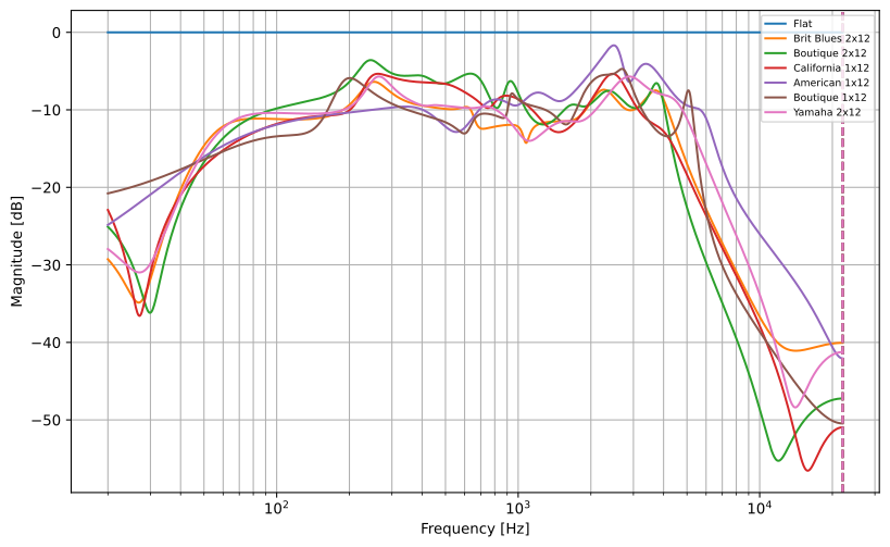
This explained why using the “flat” cabinet was much louder than the others. After all, it wasn’t intended as a selectable option and it isn’t supported by the official THR Editor software.
I realized that I could fix the volume issue by just changing the gain for cabinet type 0 from 0 to -10.
patch 0x2074318 .short -10 /* fix cabinet 0 ("flat") gain */
After making all these changes, I rebuilt the firmware with my new code and patches.
Flashing the new firmware
Now that I had a custom firmware image, I needed to find a way to
flash it onto the device. The flash chip on the device is a 2 MiB
Eon EN29LV160CB-70TIP. According to the datasheet,
it implements the Common Flash Interface (CFI). OpenOCD has support
for CFI flash, so I just needed to configure it in thr10.cfg.
flash bank thr10.flash cfi 0x2000000 0x200000 2 2 ssp2.cpu
After restarting OpenOCD, I was happy to see it detect the flash properly.
(gdb) monitor flash info 0
#0 : cfi at 0x02000000, size 0x00200000, buswidth 2, chipwidth 2
	#  0: 0x00000000 (0x4000 16kB) not protected
	#  1: 0x00004000 (0x2000 8kB) not protected
	#  2: 0x00006000 (0x2000 8kB) not protected
	#  3: 0x00008000 (0x8000 32kB) not protected
	#  4: 0x00010000 (0x10000 64kB) not protected
	#  5: 0x00020000 (0x10000 64kB) not protected
	#  6: 0x00030000 (0x10000 64kB) not protected
	#  7: 0x00040000 (0x10000 64kB) not protected
	#  8: 0x00050000 (0x10000 64kB) not protected
	#  9: 0x00060000 (0x10000 64kB) not protected
	# 10: 0x00070000 (0x10000 64kB) not protected
	# 11: 0x00080000 (0x10000 64kB) not protected
	# 12: 0x00090000 (0x10000 64kB) not protected
	# 13: 0x000a0000 (0x10000 64kB) not protected
	# 14: 0x000b0000 (0x10000 64kB) not protected
	# 15: 0x000c0000 (0x10000 64kB) not protected
	# 16: 0x000d0000 (0x10000 64kB) not protected
	# 17: 0x000e0000 (0x10000 64kB) not protected
	# 18: 0x000f0000 (0x10000 64kB) not protected
	# 19: 0x00100000 (0x10000 64kB) not protected
	# 20: 0x00110000 (0x10000 64kB) not protected
	# 21: 0x00120000 (0x10000 64kB) not protected
	# 22: 0x00130000 (0x10000 64kB) not protected
	# 23: 0x00140000 (0x10000 64kB) not protected
	# 24: 0x00150000 (0x10000 64kB) not protected
	# 25: 0x00160000 (0x10000 64kB) not protected
	# 26: 0x00170000 (0x10000 64kB) not protected
	# 27: 0x00180000 (0x10000 64kB) not protected
	# 28: 0x00190000 (0x10000 64kB) not protected
	# 29: 0x001a0000 (0x10000 64kB) not protected
	# 30: 0x001b0000 (0x10000 64kB) not protected
	# 31: 0x001c0000 (0x10000 64kB) not protected
	# 32: 0x001d0000 (0x10000 64kB) not protected
	# 33: 0x001e0000 (0x10000 64kB) not protected
	# 34: 0x001f0000 (0x10000 64kB) not protected

CFI flash: mfr: 0x007f, id:0x2249
qry: 'QRY', pri_id: 0x0002, pri_addr: 0x0040, alt_id: 0x0000, alt_addr: 0x0000
Vcc min: 2.7, Vcc max: 3.6, Vpp min: 0.0, Vpp max: 0.0
typ. word write timeout: 16 us, typ. buf write timeout: 1 us, typ. block erase timeout: 1024 ms, typ. chip erase timeout: 1 ms
max. word write timeout: 512 us, max. buf write timeout: 1 us, max. block erase timeout: 16384 ms, max. chip erase timeout: 1 ms
size: 0x200000, interface desc: 2, max buffer write size: 0x1

Spansion primary algorithm extend information:
pri: 'PRI', version: 1.0
Silicon Rev.: 0x0, Address Sensitive unlock: 0x0
Erase Suspend: 0x2, Sector Protect: 0x1
VppMin: 0.0, VppMax: 0.0

(gdb)
Now, I could flash my new image with
(gdb) monitor flash write_image erase thr10.bin 0x2010000
auto erase enabled
wrote 1048576 bytes from file thr10.bin in 13.385459s (76.501 KiB/s)
(gdb)
This only took a bit over 13 seconds, which is not bad for a compile-test cycle.
Firmware update format
I mentioned earlier that I had found a method to dump the existing firmware over USB MIDI in the same format used to update the device firmware. I wanted others to be able to apply my firmware changes to their own device without any hardware modification, so I needed to understand this format in order to produce my own firmware binaries that could be applied over USB.
The firmware dump is done by sending the following SysEx (System Exclusive) MIDI message.
00000000: f0 43 7d 50 44 54 41 31 52 4f 4d 52 02 f7 .C}PDTA1ROMR..
MIDI System Exclusive messages start with the byte F0 and end
with the byte F7. They can contain any number of 7-bit bytes
(highest bit must be unset) as a payload. These messages are commonly
used as a transport for device-specific binary protocols. In this
case, the next byte, 43, is Yamaha’s SysEx ID. I believe the next
two bytes 7D and 50 specify the device type and command code.
Following this, we have the command name DTA1ROMR, and then the
byte 02, which I think might be used to select which part of the
flash to read (the device only responds to 02).
In response, the device sends a sequence of messages starting with
00000000: f0 43 7d 30 44 54 41 31 45 52 41 53 45 02 f7 .C}0DTA1ERASE..
Here, we have the same prefix F0 43 7D, but a different command
code, 30, and name, DTA1ERASE. Again, we have the same byte
02 to select which part of the flash to erase. As the name suggests,
this erases the DTAm part of the flash in preparation for writing
the new image.
After this, there is a 16 second pause to give the erase operation time to complete.
We then receive a sequence of similarly structured DTA1MAIN
messages. Here’s the beginning and end of the first one:
00000000: f0 43 7d 40 04 0c 44 54 41 31 4d 41 49 4e 00 00  .C}@..DTA1MAIN..
00000010: 7f 7f 61 20 00 00 65 1f 70 67 14 65 1f 70 14 65  ..a ..e.pg.e.p.e
00000020: 1f 3b 70 14 65 1f 70 14 65 5d 1f 70 14 65 1f 70  .;p.e.p.e].p.e.p
00000030: 14 6e 65 1f 70 14 02 01 38 70 68 02 01 38 3c 02  .ne.p...8ph..8<.
...
000001f0: 20 40 2a 7f 7f 7b 61 30 1e 3e 01 28 20 50 0c 48   @*..{a0.>.( P.H
00000200: 20 11 00 0c 61 30 11 01 68 19 3d 40 00 24 00 20   ...a0..h.=@.$.
00000210: 04 44 10 f7                                      .D..
We have the same prefix, F0 43 7D, with command 40. However,
this time what follows is the remaining packet length (excluding
the final checksum byte, 10, and SysEx terminator, F7). We are
dealing with 7-bit bytes due to the SysEx message encoding, so the
length here is 0x04 * 0x80 + 0x0C = 524 = 0x20C.
Following this is the command name, DTA1MAIN, and then a two byte
block number, 0 in this initial block. After this is two bytes, 7F 7F. I haven’t figured out what these are for, but they’re always
the same and the updater code in the bootloader doesn’t seem to use
them.
After this comes the actual firmware data. However, we can only store 7 bits per byte in SysEx messages, so we need to figure out how the bytes are encoded.
Let’s compare the SysEx payload with the expected firmware data. The pattern starts to become clear when we group the SysEx payload into groups of 8 bytes with the last one represented in binary, and the firmware data into groups of 7 bytes.
| SysEx | 61 20 00 00 65 1F 70 1100111 14 65 1F 70 14 65 1F 0111011 70 14 65 1F 70 14 65 1011101 |
|---|---|
| Firmware | E1 A0 00 00 E5 9F F0 14 E5 9F F0 14 E5 9F F0 14 E5 9F F0 14 E5 |
We take 7 bytes of the firmware, clear their high bit, and collect the high bits into the 8th byte. This is similar to the scheme used by the file dump protocol described in the MIDI 1.0 specification, except that the byte of high bits comes after the data bytes instead of before.
A checksum is calculated over the following encoded data of this
length, and the message ends with a checksum byte, 10 for this
first block, and the usual SysEx terminator F7.
I wasn’t able to figure out the checksum algorithm by guessing, so I used Ghidra to analyze the code used to compute it. It turned out to be the lowest 7 bits of the two’s complement negation of the sum of the bytes.
Each firmware data packet is spaced 50 ms apart. After all the firmware data, we see the last message
00000000: f0 43 7d 70 44 54 41 31 43 53 55 4d 60 f7 .C}pDTA1CSUM`.
Again, the same prefix, F0 43 7D, this time with command 70,
DTA1CSUM. This is followed by an overall checksum byte, 60, and
SysEx terminator F7. The checksum is calculated the same way as
for the DTA1MAIN packets, except it’s over the entire decoded
firmware image instead of the encoded data in the packet.
I wrote two programs, bintomid and midtobin to convert between
raw binary images and the MIDI SysEx update format described above,
using the Standard MIDI Files specification as a reference.
MIDI files consist of a header chunk, followed by one or more track chunks. Tracks contain a sequence of MIDI events, each containing a delta time from the previous event. To make the timing math simple, I used a delta division of 500 ticks per quarter-note and 120 BPM. This way, each tick corresponds to 1 millisecond.
Now, I could just use millisecond delays in the event deltas. 16000
for the first DTA1MAIN message, and 50 for each subsequent message.
I added a rule to the Makefile to build a MIDI update file from
the resulting raw firmware.
Applying the update
Now that I had a firmware update file with my changes, I could update the device using the normal update procedure:
- Start the amp in update mode by turning it on while holding the
TAP button, pressing it 5 times, and then waiting for
Uto appear on the LED display. - Connect the amp to a computer over USB.
- “Play” the update MIDI file to the amp, for example using
aplaymidi -p THR10 thr10.mid.
Easy!
Future directions
While I’ve accomplished my initial goals, I still have a bunch of ideas I may want to pursue in the future.
MIDI 2 property exchange
As I’ve been messing around with my music gear, I’ve noticed that each one implements their own undocumented MIDI protocol for interacting with it and changing controls.
With MIDI 2, there is now a standard way to do this using property
exchange. It would be really nice to implement this in my amp, as
well as a generic CLI to to set and get parameters like m2 set /chorus/depth 0.4. This might also work well as a 9p filesystem.
Custom DSP effects
While I’ve only scratched the surface of the DSP-related code in my amp, I think it’d be really cool to try to understand this at a deeper level and implement my own effects. For example, an envelope filter would be really neat.
I’m not sure how to go about this. I’ve read that the SSP2 might use an SH core for the DSP, but I haven’t found anything yet that looks like SH code in the firmware. So far, I’ve found data that looks a like 8-band EQ filter coefficients for the speaker simulation, but not the DSP code that implements this filter.
I did find that the firmware MIDI code contains a developer SysEx method for writing to a DSP IO address, so I think it should be possible to develop this entirely on a separate computer, and build it into the firmware once it’s working.
Combined “mega-firmware”
There are actually three amps in the THR10 family. I have the low-gain THR10c, but there is also the standard THR10 and high-gain THR10x. Each one has a selection of five different amp models. The hardware is identical among the three amps; it’s just the firmware that’s different. There is plenty of room in the flash, so it should be possible to construct a Frankenstein firmware containing all the amp models.
I’ve looked a bit at the code related to amp modeling, and it is mostly self-contained. It should be possible to transplant by identifying common firmware functions that the block uses, and patch calls to those functions to use equivalent one in the main firmware.
I’m not sure exactly how the panel UI would look, but that should be a solvable problem.
Overall thoughts
I had a ton of fun on this project. One of the reasons I love open source so much is that I have the ability to change software to work the way I want. On the other hand, most hardware I bought felt like a black box. If I wanted to change something I was out of luck. After this project, I learned that it is possible to change how your hardware behaves; you just have to be very determined (and a bit stubborn).
This project was very satisfying since I went into it without knowing if I’d succeed or how I’d even go about attempting it. There was a lot of head banging and staring at jibberish code for hours, which made it all the more rewarding when things started to click. Sometimes it’s worth it to take on a challenge like this, even if you think you might fail. You might surprise yourself and learn a lot in the process.
The source code and tools used for this project can be found at https://github.com/michaelforney/thr10.